
This website describes the design of the Cray-1 central processor and explains how the HASE simulation model works. The model contains three demonstration programs, all held in a Programs entity. The GLOBALS parameter Program can be edited after the model has been loaded into HASE, allowing the user to choose which of the programs to run.
This Cray 1 model was originally built as an MSc project by Helen Berringer in 1998. It has since been considerably revised by Roland Ibbett.
Much of the description of the Cray-1 given here is taken from [2] which itself drew heavily on the material provided in the Cray1 Hardware Reference Manual [1]. (To avoid tortuous grammatical constructs, much of the description is written in the present tense, even though there are no longer any real Cray-1s in operation.)
The model files be downloaded from cray1_v2.1.zip.
Instructions on how to use HASE models can be found at Using HASE Models.
the second instruction uses different registers and a different functional unit from the first and can be issued one clock period after the first instruction. Subsequent to the pipeline start-up delays in the functional units (each of which can carry out operations at a rate of one per clock period), a floating-point result will appear from both the adder and the multiplier in each successive clock period. Thus if performance is estimated in terms only of floating-point addition and multiplication, the maximum floating-point execution rate is 2 FLOPS/CLOCK. Furthermore, around 60 other instructions can be issued before these units require further instructions to keep them busy. With a clock period of 12.5 ns, 2 FLOPS/CLOCK corresponds to 160 MFLOPS.
The other serious bottleneck in the CDC 7600 architecture was the entry of results into the X registers, which was also limited to one per clock period. In the Cray-1 each vector register has its own input multiplexer circuitry for selecting results from among the seven functional units which can produce vector results and, correspondingly, each vector functional unit has its own input multiplexers for selecting vector register operands. Without these circuits the Cray-1 would also be limited to 1 FLOP/CLOCK.
The overall design of the Cray-1 processor is shown in Figure 1. In addition to the eight 64-element V registers, there are eight 64-bit S (scalar) registers and eight 24-bit A (address) registers (corresponding to the X and A registers in the CDC 6600 and 7600), together with 64 B registers (each of 24 bits) and 64 T registers (each of 64 bits). The B and T registers are used in a different way from any of the registers in the 6600 and 7600, however, in that they act as buffer stores for A and S register values, respectively. The functional units take their input operands from the A, S and V registers only, and only return results to these registers.
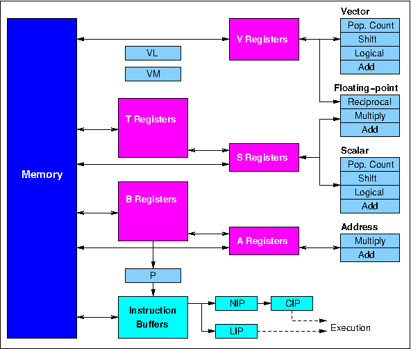
Figure 1. Cray-1 processor organisation
The A registers are used primarily as address and index registers for scalar and vector memory references, but are also used for loop control, input-output operations and to provide values for shift counts. An A register can be loaded either from a B register or direct from memory, while the B register contents can be transferred to or from memory in block copy operations which proceed at a rate of one per clock period. The S registers contain scalar operands, which may be used in scalar operations in the same way that X register values are used in the 6600 and 7600, but an S register in the Cray-1 may also supply a scalar value required for a vector operation. S register values may be transferred to or from memory or the T registers, the latter allowing intermediate results of complex computations to be held in fast buffers rather than main memory. T register values can be transferred to or from memory in the same way as B register values.
The instruction format used in the Cray-1 (Figure 2) is very similar to that used in the CDC 6600 and 7600, except that the major function field (g) contains four bits rather than three, and instructions are therefore 16 or 32 bits long rather than 15 or 30. The extra function bit allows vector as well as scalar operations to be specified, and a typical vector instruction takes the form:
implying that successive elements of Vk are to be added to successive elements of Vj, and the results returned as successive elements of Vi. Instructions which cause the transfer of an operand between A and B or S and T registers use the combined j and k fields to specify the B or T register. The j and k fields are also combined to produce shift counts in shift instructions. Instructions are issued by the control logic associated with the CIP (Current Instruction Parcel) register. In the case of a 2-parcel (32-bit) instruction, the m field is taken from the LIP (Lower Instrucion Parcel) register, which is filled from the Instruction Buffers concurrently with the NIP (Next Instruction Parcel) register.
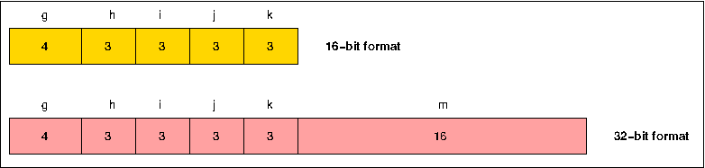
Figure 2. Cray-1 instruction formats
In addition to the operating and buffer registers, the Cray-1 processor also contains several additional registers which support the control of program execution: the program counter (P), the Vector Mask register (VM) and the Vector Length register (VL). The VM register contains 64 bits, one per element position in the vector registers. In merge operations each bit in VM is used to select the corresponding element of one or other source vector for copying into the destination vector, while in test operations bits in VM are set according to whether or not corresponding elements in a source vector satisfy the chosen condition. The VL register contains a number in the range 0 to 64 and determines how many vector elements take part in an operation. In the case of an operation on a 150-element vector, for example, the hardware would be required to treat this as two successive 64-element operations (with VL = 64) followed by a 22-element operation (with VL = 22).
Also shown are two entities that form part of the model rather than the Cray-1 itself, i.e. the standard HASE Clock entity and the Programs entity. The Programs entity contains two arrays, one for instructions and one for (integer) data. Because memories in HASE are implemented as C++ arrays, the type-checking in C++ means that it is not possible to mix different types of element in a single array. The Memory has therefore been implemented as an array of 16-character hexadecimal words and at the start of a simulation the contents of the two arrays in the Progam entity are converted into 16-character hexadecimal format and copied into the Memory.
The Programs entity allows users to create code in readable Cray-1 format while keeping the Memory as a single array (in most other HASE models, the memories are implemented using separate arrays for code and data). The problem of floating-point remains, however, as in other HASE models. In principle, users could convert all their code and data into 16-character hexadecimal format, thus allowing instructions, fixed-point (integer) values and floating-point (real) values all to be held in the single Memory, but in the current version of the model, the presence of the Programs entity means that only integer data values are allowed.
When downloaded, the Programs entity contains three programs, held in
the PROGRAMS.prog_mem.mem file. After loading the project,
the user can choose which program to run by editing the GLOBALS
parameter Program and updating the model's parameter file by
clicking the "Write Parameters" button
![]() .
Users can add a program of their own, as Program 4, in
the PROGRAMS.prog_mem.mem file, starting at locations 1536.
Program 1 requires no data and Programs 2 and 3 use the same data held
in the PROGRAMS.data_mem.mem file. Users can add their own
data to this file at locations beyond the existing data but must
ensure that their program selects this data from those locations.
.
Users can add a program of their own, as Program 4, in
the PROGRAMS.prog_mem.mem file, starting at locations 1536.
Program 1 requires no data and Programs 2 and 3 use the same data held
in the PROGRAMS.data_mem.mem file. Users can add their own
data to this file at locations beyond the existing data but must
ensure that their program selects this data from those locations.
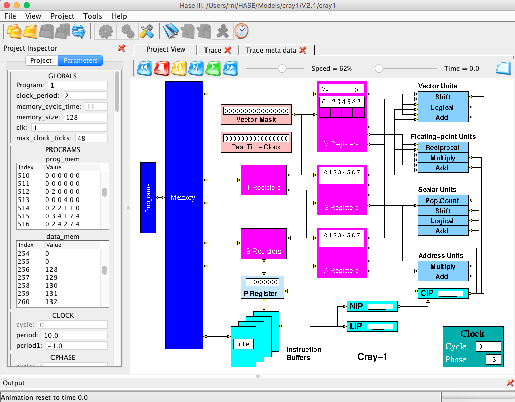
Figure 3. Cray-1 simulation model loaded into HASE
Once a trace file has been loaded, the animation control icons at the
top of the Project View pane become active, as shown in Figure 4. From
left to right, these allow the animation to be rewound, stopped,
paused, single stepped, run or fast forwarded to the end. As the
animation proceeds, packets of information can be seen passing between
entities while the entities themselves change colour to reflect their
states (idle, busy, waiting). The vector registers (individually
identified as small rectangles) can be in one of three states:
idle ![]() ,
reserved
,
reserved ![]() ,
chained
,
chained ![]() .
Right clicking on one of these vector register icons pops the
corresponding register contents list out of the Project Inspector
pane, as it does for the A, B, S and T registers. Demonstration
Program 3, described below, shows how the chaining mechanism
operates.
.
Right clicking on one of these vector register icons pops the
corresponding register contents list out of the Project Inspector
pane, as it does for the A, B, S and T registers. Demonstration
Program 3, described below, shows how the chaining mechanism
operates.
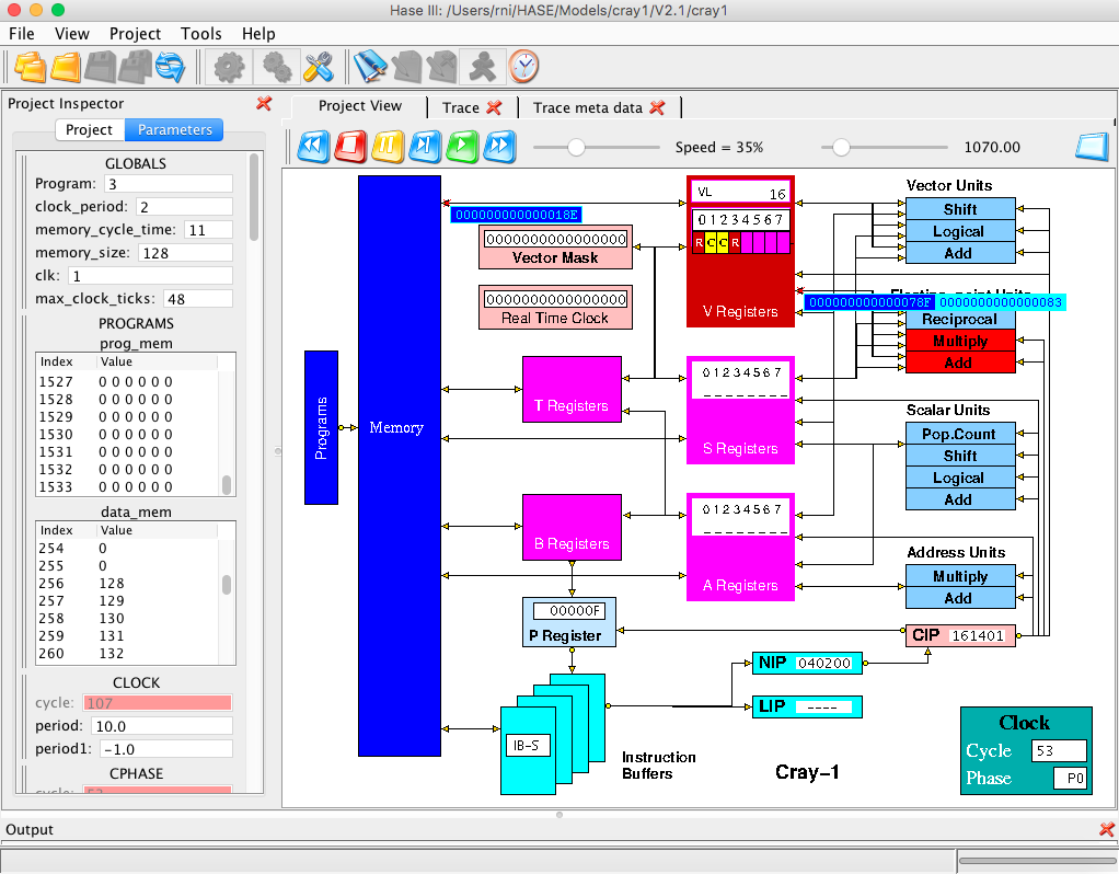
Figure 4. Cray-1 simulation model during animation
Table 1 shows the full instruction set of the Cray-1. Not all of them are implemented in the HASE model; those that are implemented have their octal code shown in red. Most of those that are not (shown in blue) have been omitted because they are specific to the implementation of floating-point numbers. More instructions may be implemented in future versions.
|
|
Table 1. Cray 1 instruction set
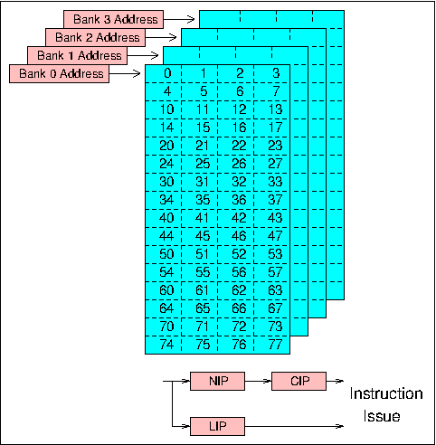
Figure 5. Cray-1 Instruction Buffers
The Cray-1 has a 22-bit instruction address and the first instruction parcel in a buffer always has an address starting on a 64-parcel address boundary. Any one buffer is therefore defined by the 16 most significant bits of a parcel address, and for each buffer there is a 16-bit Bank Address Register containing this value. At each clock cycle the high order bits of the program address counter are compared with the contents of these registers. If a match occurs the required instruction parcel is selected from within the appropriate buffer either immediately, if the buffer concerned is the same as the one which supplied the previous parcel, or after a two clock period delay if a change of buffers is involved.
If no match occurs, instructions must be loaded into one of the instruction buffers before execution can continue. A two-bit counter is used to determine which buffer is to be loaded; this counter is incremented by one whenever a load operation occurs, thus implementing a cyclic replacement algorithm. The 64-bit main store in the Cray-1 is an 8-way or 16-way interleaved bipolar semiconductor store having a 50 ns cycle time. During a block transfer all other store requests are inhibited, and sequential accesses can be made at a rate of one per 12.5 ns clock period. In the case of transfers to an instruction buffer, four storage banks can be accessed in parallel, giving access to 16 instruction parcels in one cycle and allowing all 16 banks in a 16-bank configuration to be accessed in four clock periods. Since the cycle time is also equal to four clock periods, the first four banks are then ready to accept a further request, and a complete block transfer to an instruction buffer occupies four cycles of each bank. The total time required to access the first group of instruction parcels is nevertheless quite long, and a 14 clock period delay is incurred whenever a buffer has to be loaded. This delay is constant regardless of the position of the first parcel required from the buffer, so the first group of 16 parcels delivered to the buffers is always the one required immediately by the processor. Subsequent groups arrive at a rate of 16 parcels per clock period and fill the buffer circularly.
When a branch is taken the new value in the program address counter is compared with the contents of the buffer starting address registers in exactly the same way as it is following execution of instructions in sequence. If a match occurs the required instruction is selected from the appropriate buffer, and if not a block transfer is initiated. Separate subroutines, or even non-contiguous segments of code within a loop, may be held concurrently in separate buffers.
To meet these requirements, the Cray-1 uses a reservation mechanism (similar to that used in the CDC 7600). When an instruction is issued that will deliver a new result to a V, S or A register, a reservation is set for that register which prevents the issuing of any subsequent instruction requiring the use of that register until the result has been delivered. In the model, the reservations on the S and A registers are displayed in two ways: (1) in the Project View pane by the presence of an "R" under the relevant register number; (2) in the CIP section of the Parameters pane by the presence of a function unit identifying letter ("A" for Add, etc) in the S_entries/A_entries queues, which show the progress of the instruction through the relevant function unit pipeline. The reservation mechanism for the V registers is more complex, as explained below in the section describing Demonstration Program 3.
The first action that occurs at the start of a simulation is the P Register sending its current value to the Instruction Buffers (effectively a branch, to location 0 in this case). Initially the Bank Address Registers are set to all 1's while the buffers themselves are all empty. The Instruction Buffers therefore send a request to Memory. When the first 16 instruction parcels arrive from Memory, they are loaded into Instruction Buffer 0 and the instruction at address 0 is sent to NIP and thence to CIP. The first 4 instructions set up values in registers A0 - A3 for use in later instructions in the progaram. The next instruction is a conditional branch instruction, for which the condition is not satisfied, so doesn't branch. This is shown to be the case by the execution of the next instruction which increments A2. The instruction after this is a conditional branch for which the condition is satisfied, so does branch, to an instruction that is not in Buffer 0. This causes a second request to Memory and the returned instructions to be loaded into Buffer 1.
Subsequent instructions check for correct branch/no branch outcomes of all the different conditional and unconditional branch instructions and for correct operation of the buffers. In Table 2 each branch from/to pair in the program is highlighted in a different colour. Entries in the IB Action column show the actions that occur in the Buffers each time P is updated by a branch instruction.
The last instruction to be executed is an 004 (normal exit) instruction that stops the simulation. The ijk fields of an 004 instruction are ignored in the Cray-1 itself but this simulation model uses the ijk value to report which instance of the 004 instruction in the program ended the simulation. In this case the report should be "Simulation stopped by 004 instruction 0". At the end of the simulation the value in A2 should be 13, while the value in A3 should be unaltered, i.e. 0.
| P | IB Action | g h i j k | Instruction | Result | |
| 00 | Fill Buffer 0 | 02 2 0 0 0 | Transmit jk to A0 | A0 = 0 | |
| 01 | 02 2 1 0 1 | Transmit jk to A1 | A1 = 1 | ||
| 02 | 02 2 2 0 0 | Transmit jk to A2 | A2 = 0 | ||
| 03 | 02 2 3 0 0 | Transmit jk to A3 | A3 = 0 | ||
| 04 | 01 1 0 0 0 | Branch to ijkm if (A0) ≠ 0 | |||
| 05 | 00 0 0 1 5 | Doesn't branch | |||
| 06 | 03 0 2 2 1 | Integer sum of (A2) and (A1) to A2 | A2 = 1 | ||
| 07 | 01 0 0 0 0 | Branch to ijkm if (A0) = 0 | |||
| 08 | 00 0 1 0 0 | Branch to P = 000040 | |||
| 09 | 03 0 3 3 1 | Integer sum of (A3) and (A1) to A3 | not executed | ||
| 0A | Same Buffer | 00 4 0 0 1 | Normal exit | Stop (1) | |
| 0B | Switch to Buffer 0 | 00 7 0 0 0 | Return jump to ijkm; set B00 to (P) | ||
| 0C | 00 0 4 0 0 | Branch to P = 000100 | |||
| 0D | Overwrite Buffer 0 | 00 6 0 0 0 | Branch to ijkm | ||
| 0E | 00 0 0 1 2 | Branch to 00000A | |||
| 0F | 00 0 0 0 0 | ||||
| ... | 00 0 0 0 0 | ||||
| 3E | 00 0 0 0 0 | ||||
| 40 | Fill Buffer 1 | 03 0 2 2 1 | Integer sum of (A2) and (A1) to A2 | A2 = 2 | |
| 41 | 01 3 0 0 0 | Branch to ijkm if (A0) negative | |||
| 42 | 00 0 0 1 5 | Doesn't branch | |||
| 43 | 03 0 2 2 1 | Integer sum of (A2) and (A1) to A2 | A2 = 3 | ||
| 44 | 01 2 0 0 0 | Branch to ijkm if (A0) positive | |||
| 45 | 00 0 2 2 6 | Branch to P = 000096 | |||
| 46 | 03 0 3 3 1 | Integer sum of (A3) and (A1) to A3 | not executed | ||
| 47 | 00 4 0 0 2 | Normal exit | Stop (2) | ||
| 48 | 00 0 0 0 0 | ||||
| ... | 00 0 0 0 0 | ||||
| 95 | 00 0 0 0 0 | ||||
| 96 | Fill Buffer 2 | 03 1 0 0 1 | Integer difference of (A0) and (A1) to A0 | A0 = -1 | |
| 97 | 03 0 2 2 1 | Integer sum of (A2) and (A1) to A2 | A2 = 4 | ||
| 98 | 01 0 0 0 0 | Branch to ijkm if (A0) = 0 | |||
| 99 | 00 0 0 1 5 | Doesn't branch | |||
| 9A | 03 0 2 2 1 | Integer sum of (A2) and (A1) to A2 | A2 = 5 | ||
| 9B | 01 1 0 0 0 | Branch to ijkm if (A0) ≠ 0 | |||
| 9C | 00 0 3 0 0 | Branch to P = 0000C0 | |||
| 9D | 03 0 3 3 1 | Integer sum of (A3) and (A1) to A3 | not executed | ||
| 9E | 00 4 0 0 3 | Normal exit | Stop (3) | ||
| 9F | 00 0 0 0 0 | ||||
| ... | 00 0 0 0 0 | ||||
| BF | 00 0 0 0 0 | ||||
| C0 | Fill Buffer 3 | 03 0 2 2 1 | Integer sum of (A2) and (A1) to A2 | A2 = 6 | |
| C1 | 01 2 0 0 0 | Branch to ijkm if (A0) positive | |||
| C2 | 00 0 0 1 5 | Doesn't branch | |||
| C3 | 03 0 2 2 1 | Integer sum of (A2) and (A1) to A2 | A2 = 7 | ||
| C4 | 01 3 0 0 0 | Branch to ijkm if (A0) negative | |||
| C5 | 00 0 0 1 3 | Branch to P = 00000B | |||
| C6 | 03 0 3 3 1 | Integer sum of (A3) and (A1) to A3 | not executed | ||
| C7 | 00 4 0 0 4 | Normal exit | Stop (4) | ||
| C8 | 00 0 0 0 0 | ||||
| ... | 00 0 0 0 0 | ||||
| FF | 00 0 0 0 0 | ||||
| 100 | Overwrite Buffer 0 | 04 0 0 0 0 | Transmit jkm to Si | ||
| 101 | 00 0 0 0 0 | S0 = 0 | |||
| 102 | 04 0 1 0 0 | Transmit jkm to Si | |||
| 103 | 00 0 0 0 1 | S1 = 1 | |||
| 104 | 01 5 0 0 0 | Branch to ijkm if (S0) ≠ 0 | |||
| 105 | 00 0 0 1 5 | Doesn't branch | |||
| 106 | 03 0 2 2 1 | Integer sum of (A2) and (A1) to A2 | A2 = 8 | ||
| 107 | 01 6 0 0 0 | Branch to ijkm if (S0) = 0 | |||
| 108 | 00 0 5 0 0 | Branch to P = 000140 | |||
| 109 | 03 0 3 3 1 | Integer sum of (A3) and (A1) to A3 | not executed | ||
| 10A | 00 4 0 0 5 | Normal exit | Stop (5) | ||
| 10B | 00 0 0 0 0 | ||||
| ... | 00 0 0 0 0 | ||||
| 13F | 00 0 0 0 0 | ||||
| 140 | Overwrite Buffer 1 | 03 0 2 2 1 | Integer sum of (A2) and (A1) to A2 | A2 = 9 | |
| 141 | 01 7 0 0 0 | Branch to ijkm if (S0) negative | |||
| 142 | 00 0 0 1 5 | Doesn't branch | |||
| 143 | 03 0 2 2 1 | Integer sum of (A2) and (A1) to A2 | A2 = 10 | ||
| 144 | 01 6 0 0 0 | Branch to ijkm if (S0) positive | |||
| 145 | 00 0 6 0 0 | Branch to P = 000180 | |||
| 146 | 03 0 3 3 1 | Integer sum of (A3) and (A1) to A3 | not executed | ||
| 147 | 00 4 0 0 6 | Normal exit | Stop (6) | ||
| 148 | 00 0 0 0 0 | ||||
| ... | 00 0 0 0 0 | ||||
| 17F | 00 0 0 0 0 | ||||
| 180 | Overwrite Buffer 2 | 06 1 0 0 1 | Integer difference of (Sj) and (Sk) to Si | S0 = -1 | |
| 181 | 01 4 0 0 0 | Branch to ijkm if (S0) = 0 | |||
| 182 | 00 0 0 1 5 | Doesn't branch | |||
| 183 | 03 0 2 2 1 | Integer sum of (A2) and (A1) to A2 | A2 = 11 | ||
| 184 | 01 5 0 0 0 | Branch to ijkm if (A0) ≠ 0 | |||
| 185 | 00 0 7 0 0 | Branch to P = 0001C0 | |||
| 186 | 03 0 3 3 1 | Integer sum of (A3) and (A1) to A3 | not executed | ||
| 187 | 00 4 0 0 7 | Normal exit | Stop (7) | ||
| 188 | 00 0 0 0 0 | ||||
| ... | 00 0 0 0 0 | ||||
| 1BF | 00 0 0 0 0 | ||||
| 1C0 | Overwrite Buffer 3 | 03 0 2 2 1 | Integer sum of (A2) and (A1) to A2 | A2 = 12 | |
| 1C1 | 01 6 0 0 0 | Branch to ijkm if (S0) positive | |||
| 1C2 | 00 0 0 1 5 | Doesn't branch | |||
| 1C3 | 03 0 2 2 1 | Integer sum of (A2) and (A1) to A2 | A2 = 13 | ||
| 1C4 | 01 7 0 0 0 | Branch to ijkm if (S0) negative | |||
| 1C5 | 00 0 7 0 7 | Branch to P = 0001C7 | |||
| 1C6 | 03 0 3 3 1 | Integer sum of (A3) and (A1) to A3 | not executed | ||
| 1C7 | Same Buffer | 00 5 0 0 0 | Branch to Bjk | Branch to P = 00000D |
Table 2. Demonstration Program 1
Transfers between the B/T registers and the A/S registers use the i field to select the A/S register and jk to select the B/T register. Transfers to/from the Vector Mask (VM) register use the j/i field respectively to select an S register.
The fourth unit in this group is the Population and Leading Zero Count Unit which takes a 64-bit operand from an S register and returns a 7-bit result, equal to the number of ones in the operand or the number of zeros preceding the most significant 1 in the operand, to an A register. The first of these operations requires four clock periods for its execution, and the second three.
| P | g h i j k | Instruction | Result |
| Integer values are shown in black, hexadecimal values in blue | |||
| 00 | 02 0 0 0 0 | Transmit jkm to A0 | |
| 01 | 00 0 4 0 0 | m field | A0 = 256 |
| 02 | 02 2 1 1 0 | Transmit jk to A1 | A1 = 8 |
| 03 | 03 4 1 7 4 | Block transfer: Memory to B registers | B60-63 = 128-131, B00-03 = 132-135 |
| 04 | 02 4 2 7 4 | Transmit (B60) to A2 | A2 = 128 |
| 05 | 02 4 3 7 5 | Transmit (B61) to A3 | A3 = 129 |
| 06 | 03 2 4 2 3 | Integer product of (A2) and (A3) to A4 | A4 = 16512 |
| 07 | 03 0 5 0 3 | Integer sum of (A0) and (A3) to A5 | A5 =129 [A0 = 0] |
| 08 | 03 0 6 4 0 | Integer sum of (A4) and (A0) to A6 | A6 =16513 [A0 = 1] |
| 09 | 03 0 7 4 5 | Integer sum of (A4) and (A5) to A7 | A7 =16641 |
| 0A | 02 5 6 0 4 | Transmit (A6) to B04 | B04 = 16513 |
| 0B | 02 5 7 0 5 | Transmit (A7) to B05 | B05 =16641 |
| 0C | 02 1 4 0 1 | Transmit ~jkm to A4 | |
| 0D | 00 0 0 7 1 | m field | A4 = -65594 |
| 0E | 02 5 4 0 6 | Transmit (A4) to B06 | B06 = -65594 |
| 0F | 03 1 4 7 6 | Integer difference of (A7) and (A6) to A4 | A4 = 128 |
| 10 | 02 5 4 0 7 | Transmit (A4) to B07 | B07 = 128 |
| 11 | 04 0 1 0 0 | Transmit jkm to S1 | |
| 12 | 00 0 0 0 1 | m field | S1 = 1 |
| 13 | 04 0 2 5 2 | Transmit jkm to S2 | |
| 14 | 01 0 5 7 5 | m field | S2 = 2756989 |
| 15 | 04 1 3 0 0 | Transmit ~jkm to S3 | |
| 16 | 00 0 0 0 1 | m field | S3 = -2 |
| 17 | 02 6 1 1 0 | Population count of S1 to A1 | A1 = 1 |
| 18 | 02 7 2 1 0 | Leading zero count of S1 to A2 | A2 = 63 |
| 19 | 02 6 3 2 0 | Population count of S2 to A3 | A3 = 11 |
| 1A | 02 7 4 2 0 | Leading zero count of S2 to A4 | A4 = 42 |
| 1B | 02 6 5 3 0 | Population count of S3 to A5 | A5 = 63 |
| 1C | 02 7 6 3 0 | Leading zero count of S3 to A6 | A6 = 0 |
| 1D | 02 3 7 2 0 | Transmit S2 to A7 | A7 = 2756989 |
| 1E | 02 5 1 1 0 | Transmit (A1) to B08 | B08 = 1 |
| 1F | 02 5 2 1 1 | Transmit (A2) to B09 | B09 = 63 |
| 20 | 02 5 3 1 2 | Transmit (A3) to B10 | B10 = 11 |
| 21 | 02 5 4 1 3 | Transmit (A4) to B11 | B11 = 42 |
| 22 | 02 5 5 1 4 | Transmit (A5) to B12 | B12 = 63 |
| 23 | 02 5 6 1 5 | Transmit (A6) to B13 | B13 = 0 |
| 24 | 02 5 7 1 6 | Transmit (A7) to B14 | B14 = 2756989 |
| 25 | 02 0 0 0 0 | Transmit jkm to A0 | |
| 26 | 00 0 6 0 0 | m field | A0 = 384 |
| 27 | 02 2 1 1 3 | Transmit 11 to A1 | A1 = 11 |
| 28 | 03 5 1 0 4 | Block transfer: B registers to Memory | M[384-394] = (B04-14) |
| 29 | 02 0 0 0 0 | Transmit jkm to A0 | |
| 2A | 00 0 4 1 5 | m field | A0 = 269 |
| 2B | 02 2 1 0 4 | Transmit jk to A1 | A1 = 4 |
| 2C | 03 6 1 0 0 | Block transfer: Memory to T registers | T00-03 = 141, 142, 143, 256 |
| 2D | 07 4 0 0 0 | Transmit (T00) to S0 | S0 = 141 |
| 2E | 07 4 1 0 1 | Transmit (T01) to S1 | S1 = 142 |
| 2F | 06 0 3 0 1 | Integer sum of (S0) and (S1) to S3 | S3 = 142 [S0 = 0] |
| 30 | 07 4 2 0 2 | Transmit (T02) to S2 | S2 = 143 |
| 31 | 06 0 4 1 2 | Integer sum of (S1) and (S2) to S4 | S4 = 285 |
| 32 | 06 1 5 3 4 | Integer difference of (S3) and (S4) to S5 | S5 = -143 |
| 33 | 07 5 3 1 0 | Transmit (S3) to T08 | T08 = 142 |
| 34 | 07 5 4 1 1 | Transmit (S4) to T09 | T09 = 285 |
| 35 | 07 5 5 1 2 | Transmit (S5) to T10 | T10 = -143 |
| 36 | 04 0 1 2 5 | Transmit jkm to S1 | |
| 37 | 25 2 5 2 5 | m field | S1 = 0000000000155555 |
| 38 | 05 1 2 0 1 | Logical sum of (S0) and (S1) to S2 | S2 = 0000000000155555 [S0 = 0] |
| 39 | 05 4 2 2 6 | Shift (S2) left 22 places to S2 | S2 = 0000055555400000 |
| 3A | 05 1 2 2 1 | Logical sum of (S2) and (S1) to S2 | S2 = 0000055555555555 |
| 3B | 05 4 2 2 6 | Shift (S2) left 22 places to S2 | S2 = 5555555555400000 |
| 3C | 05 1 2 2 1 | Logical sum of (S2) and (S1) to S2 | S2 = 5555555555555555 |
| 3D | 00 3 0 2 0 | Transmit (S2) to vector mask | VM = 5555555555555555 |
| 3E | 07 3 3 0 0 | Transmit (VM) to S3 | S3 = 1431655765 |
| 3F | 05 3 3 3 0 | Shift S3 right 64-24 places to S0 | S0 = 5592405 |
| 40 | 05 5 3 2 1 | Shift S3 right 64-17 places to S3 | S3 = 000000000000AAAA |
| 41 | 07 5 0 1 3 | Transmit (S0) to T11 | T11 = 5592405 |
| 42 | 07 5 3 1 4 | Transmit (S3) to T12 | T12 = 170 |
| 43 | 05 2 4 0 4 | Shift (S4) left jk places to S0 | S0 = 4560 |
| 44 | 07 5 0 1 5 | Transmit (S0) to T13 | T13 = 4560 |
| 45 | 04 2 1 6 3 | Form 64-51 bits of 1's mask in S1 from right | S1 = 0000000000001FFF |
| 46 | 04 3 2 6 6 | Form 54 bits of 1's mask in S2 from left | S2 = -1024 |
| 47 | 04 4 4 1 3 | Logical product of (S1) and (S3) to S4 | S4 = 0000000000000AAA |
| 48 | 04 5 5 1 3 | Logical product of (S1) and ~(S3) to S5 | S5 = 0000000000001555 |
| 49 | 04 6 6 1 3 | Logical difference of (S1) and (S3) to S6 | S6 = 000000000000B555 |
| 4A | 04 7 7 1 3 | Logical equivalence of (S1) and (S3) to S7 | S7 = FFFFFFFFFFFF4AAA |
| 4B | 07 5 1 1 6 | Transmit (S1) to T14 | T14 = 8191 |
| 4C | 07 5 2 1 7 | Transmit (S2) to T15 | T15 = -1024 |
| 4D | 07 5 3 2 0 | Transmit (S3) to T16 | T16 = 43690 |
| 4E | 07 5 4 2 1 | Transmit (S4) to T17 | T17 = 2730 |
| 4F | 07 5 5 2 2 | Transmit (S5) to T18 | T18 = 5461 |
| 50 | 07 5 6 2 3 | Transmit (S6) to T19 | T19 = 46421 |
| 51 | 07 5 7 2 4 | Transmit (S7) to T20 | T20 = -46422 |
| 52 | 02 0 0 0 0 | Transmit jkm to Ai | |
| 53 | 00 0 6 2 0 | m field | A0 = 400 |
| 54 | 02 2 1 1 5 | Transmit jk to A1 | A1 = 13 |
| 55 | 03 7 1 1 0 | Block Transfer (A1) T registers to memory | M[400-412] = (T08-20) |
| 56 | 10 2 6 0 0 | Read from ((A2) + jkm) to A6 | |
| 57 | 00 0 3 5 3 | m field | A6 = M[298] = 394 |
| 58 | 11 6 7 0 0 | Store (A7) to (A6) + jkm | |
| 59 | 00 0 0 0 1 | m field | M[395] = 2A117D |
| 5A | 12 2 6 0 0 | Read from ((A2) + jkm) to S1 | |
| 5B | 00 0 3 5 4 | m field | S1 = M[299] = 395 |
| 5C | 13 6 7 0 0 | Store (S7) to (A6) + jkm | |
| 5D | 00 0 0 0 2 | m field | M[396] = FFFFFFFFFFFF4AAA |
| 5E | 00 4 0 0 0 | Stop | |
Table 3. Demonstration Program 2
The only other exception to these reservation requirements occurs when an element value which is being delivered to a vector register can, in the same clock period, be routed to another functional unit as an input operand. This arrangement allows chaining of vector operations. Chaining starts when a match occurs between one of the V register operand designators of an instruction awaiting issue in CIP, and the V register result designator of a previously issued instruction which has not yet returned its first result element. When this element becomes available for delivery to the result register, the instruction in CIP is issued (provided there are no other hold-ups) and the result element is forwarded with this instruction to the appropriate functional unit. Successive elements follow until the whole vector has been both written into its result register and forwarded to the second functional unit. The results of this second vector operation may themselves be chained into a third operation, and so on, as shown in the following example:
Assuming that VL is set to 64, the first instruction causes 64 operands from a designated area in memory to be read out and copied in sequence into the 64 element positions in V0. Store requests are pipelined in such a way that the store appears to the processor as a pseudo functional unit. Thus after a start-up delay of seven clock periods, the first element of the vector from store becomes available for delivery to V2, and successive elements follow in successive clock periods.
The second instruction can only be issued once the first instruction has completed because only one vector element at a time can be read from Memory. In the clock period following the issue of the second instruction, the third instruction in the sequence is copied into CIP, but the reservation on V1 prevents it from being issued immediately. This reservation is lifted, however, allowing the instruction to issue, during the clock period in which the first vector element arrives from Memory ready for delivery to V1. This clock period is known as chain slot time. Chaining allows the vector elements being copied into V1 to flow directly from the memory read pipeline into the Floating-point Multiply Unit pipeline, where each element is multiplied by the value taken from S1 at the start of the operation, to produce the vector V2.
The fourth instruction in the sequence becomes ready for issue in the clock period following issue of the third instruction, and it too is held up by a reservation on one of its input operands, this time V2. When the first element of V2 appears from the Floating-point Multiply Unit, the reservation on V2 is lifted, allowing this fourth instruction to issue. Now the elements emanating from the Floating-point Multiply Unit can flow directly into the Floating-point Add Unit pipeline as well as into the result register V2. Thus the memory read pipeline, and the Floating-point Multiply and Floating-point Add Unit pipelines are all chained together to produce the elements of V3. One of the reasons why this works is that the memory and the functional units can each deliver a new result in each successive clock period. In Program 3 in the model, the instruction at P = 02 sets VL to 16 (to avoid the tedium of watching 64-element operations), while the 4 instructions described above are at P = 05 and P = 0A - 0C. The instructions at P = 06 - 09 can proceed whilst the transfer from Memory to V1 is in progress, since they don't involve any Memory accesses. Likewise, the instruction at P = 0D, which sets A0 equal to the Memory start address for the subsequent block transfer of V5 to Memory, can proceed whilst the floating sums operation is in progress, but the block transfer itself cannot be chained to the floating sums operation because the first action of a block transfer instruction, at chain slot time, is the transfer of the start address in A0 to the Vector Registers, not the first transfer of a data value to Memory.
| P | g h i j k | Instruction | Result |
| Integer values are shown in black, hexadecimal values in blue | |||
| 00 | 02 2 1 2 0 | Transmit jk to A1 | A1 = 16 |
| 01 | 02 2 2 0 1 | Transmit jk to A2 | A2 = 1 |
| 02 | 00 2 0 0 1 | Transmit (A1) to VL | VL = 16 |
| 03 | 02 0 0 0 0 | Transmit jkm to A0 | |
| 04 | 00 0 4 0 0 | m field | A0 = 256 |
| 05 | 17 6 0 0 2 | Block transfer: Memory[256-271] to V0 |
V0 = 128, 129, 130, 131, 132, 133, 134, 135, 136, 137, 138, 139, 140, 141, 142, 143 |
| 06 | 04 0 1 0 0 | Transmit jkm to S1 | |
| 07 | 00 0 0 0 5 | m field | S1 = 5 |
| 08 | 02 0 0 0 0 | Transmit jkm to A0 | |
| 09 | 00 0 4 4 0 | m field | A0 = 272 |
| 0A | 17 6 1 0 2 | Block transfer: Memory[272-287] to V1 |
V1 = 384, 385, 386, 387, 388, 398, 390, 391, 392, 393, 394, 395, 396, 397, 398, 399 |
| 0B | 16 0 2 1 1 | Floating products (S1) and (V1) to V2 (V1 chained) |
V2 = 1920, 1925, 1930, 1935, 1940, 1945, 1950, 1955, 1960, 1965, 1970, 1975, 1980, 1985, 1990, 1995 |
| 0C | 17 1 3 2 0 | Floating sums (V2) and (V0) to V3 (V2 chained) |
V3 = 2048, 2054, 2060, 2066, 2072, 2078, 2084, 2090, 2096, 2102, 2108, 2114, 2120, 2126, 2132, 2138 |
| 0D | 16 1 4 0 1 | Floating products (V0) and (V1) to V4 |
V4 = 49152, 49665, 50180, 50697, 51216, 51737, 52260, 52785, 53312, 53841, 54372, 54905, 55440, 55977, 56516, 57057 |
| 0E | 04 0 2 0 0 | Transmit jkm to S2 | |
| 0F | 15 0 1 0 0 | m field | S2 = 53312 |
| 10 | 17 2 5 2 4 | Floating differences (S2) and (V4) to V5 (V4 chained) |
V5 = 4160, 3647, 3132, 2615, 2096, 1575, 1052, 527, 0, -529, -1060, -1593, -2128, -2665, -3204, -3745 |
| 11 | 02 0 0 0 0 | Transmit jkm to A0 | |
| 12 | 00 0 6 2 0 | m field | A0 = 384 |
| 13 | 17 7 0 5 2 | Block transfer: V5 to Memory (Can't be chained) |
Memory[384-399] = (V5) |
| 14 | 04 0 2 0 0 | Transmit jkm to S2 | |
| 15 | 00 3 6 3 6 | m field | S2 = 1950 |
| 16 | 17 0 6 3 0 | Floating sums (S3) and (V0) to V6 |
V6 = 2078, 2079, 2080, 2081, 2082, 2083, 2084, 2085, 2086, 2087, 2088, 2089, 2090, 2091, 2092, 2093 |
| 17 | 02 0 0 0 0 | Transmit jkm to A0 | |
| 18 | 00 0 5 0 0 | m field | A0 = 320 |
| 19 | 17 6 0 0 2 | Block transfer: Memory[320-335] to V0 |
V0 = 42, -56, 0, -27, 17, 0, -48, 0, 89, 0, 127, -96, 0, -45, 74, -25 |
| 1A | 17 5 0 0 0 | VM[e] = 1 if (V0[e]) = 0 (V0 chained) |
VM = 2548000000000000 |
| 1B | 14 7 3 1 2 | Merge (V1) and (V2) to V3 | V3 = 1920, 1925, 386, 1935, 1940, 389, 1950, 391, 1960, 393, 1970, 1975, 396, 1985, 1990, 1995 |
| 1C | 17 5 0 0 1 | VM[e] = 1 if (V0[e]) != 0 | VM = DAB7000000000000 |
| 1D | 04 0 4 0 0 | Transmit jkm to S4 | |
| 1E | 01 2 3 4 5 | m field | S4 = 5349 |
| 1F | 14 6 4 4 2 | Merge (S4) and (V2) to V4 | V4 = 5349, 5349, 1930, 5349, 5349, 1945, 5349, 1955, 5349, 1965, 5349, 5349, 1980, 5349, 5349, 5349 |
| 20 | 17 5 0 0 2 | VM[e] = 1 if (V0[e]) >= 0 | VM = ADEA000000000000 |
| 21 | 14 7 5 1 2 | Merge (V1) and (V2) to V5 | V5 = 384, 1925, 386, 1935, 388, 389, 1950, 391, 392, 393, 394, 1975, 396, 1985, 398, 1995 |
| 22 | 17 5 0 0 3 | VM[e] = 1 if (V0[e]) < 0 | VM = 5215000000000000 |
| 23 | 14 7 6 1 2 | Merge (V1) and (V2) to V6 |
V6 = 1920, 385, 1930, 387, 1940, 1945, 390, 1955, 1960, 1965, 1970, 395, 1980, 397, 1990, 399 = 780, 181, 78A, 183, 794, 799, 186, 7A3, 78A, 78D, 7B2, 18B, 7BC, 18D, 7C6, 18F |
| 24 | 15 5 7 4 5 | Integer sums of (V4) and (V5) to V7 |
V7 = 5477, 5734, 516, 5736, 5481, 522, 5739, 526, 5485, 530, 5487, 5744, 536, 5746, 5491, 5748 = 1565, 1666, 0204, 1668, 1569, 020A, 1668, 020E, 156D, 0212, 156F, 1670, 0218, 1672, 1573, 1674 |
| 25 | 04 0 5 0 0 | Transmit jkm to S5 | |
| 26 | 00 0 7 7 7 | m field | S5 = 511 1FF |
| 27 | 14 0 3 5 7 | Logical products of (S5) and (V7) to V3 |
V3 = 357, 102, 4, 104, 361, 10, 107, 14 365, 18, 367, 112, 24, 114, 371, 116 = 165, 066, 004, 068, 169, 00A, 06B, 00E 16D, 012, 16F, 070, 018, 072, 173, 074 |
| 28 | 15 7 4 5 3 | Integer differences of (V5) and (V3) to V4 (V3 chained) |
V4 = -229, 283, 126, 283, -229, 123, 283, 121, -229, 119, -229, 283, 116, 283, -229, 283 |
| 29 | 14 3 5 3 6 | Logical sums of (V3) and (V6) to V5 |
V5 = 485, 231, 390, 235, 493, 399, 239, 399, 493, 411, 495, 251, 412, 255, 511, 255 |
| 2A | 14 4 2 5 3 | Logical differences of (S5) and (V3) to V2 |
V2 = 09A, 199, 1FB, 197, 096, 1F5, 194, 1F1, 092, 1ED, 090, 18F, 1E7, 18D, 08C, 18B |
| 2B | 07 7 0 4 1 | Transmit (S4) to V0 element (A1) | V0 element 16 = 5349 |
| 2C | 07 6 3 3 2 | Transmit V3 element (A2) to S3 | S3 = V3 element 1 = 102 |
| 2D | 02 2 3 0 4 | Transmit jk to A3 | A3 = 4 |
| 2E | 15 0 6 5 3 | Single shift of (V5) left by (A3) places to V6 |
V6 = 32336, 7856, 30944, 8084, 32720, 31216, 6256, 31408, 32464, 31728, 32752, 6640, 32704, 6896, 32624, 7152 |
| 2F | 15 1 7 6 0 | Single shift of (V6) right by 1 place to V7 (shift by 1 if k = 0) |
V7 = 16168, 3928, 15472, 4024, 16360, 15608, 3128, 15704, 16232, 15864, 16376, 3320, 16352, 3448, 16312, 3576 |
| 30 | 17 4 1 7 1 | Population count of (V7) to V1 |
V1 = 8, 7, 7, 8, 10, 9, 5, 8, 9, 10, 11, 7, 9, 7, 10, 8 |
| 31 | 17 4 2 7 2 | Population count parities of (V7) to V2 |
V2 = 0, 1, 1, 0, 0, 1, 1, 0, 1, 0, 1, 1, 1, 1, 0, 0 |
| 32 | 00 4 0 0 0 | Stop | |
Table 4. Demonstration Program 3
Return to Computer Architecture Simulation Models