Computer Architecture Simulation & Visualisation
Return to Computer Architecture Simulation Models

HASE SIMD Array Processor Models
The HASE SIMD-1 and SIMD-2 simulation models are designed to show the
principles of operation of a 1-dimensional and a 2-dimensional Single
Instruction Multiple Data processing system. Each consists of a
Memory, an Array Control Unit (ACU) and an SIMD array of simple
processing elements (PEs). The models both use the same Memory, ACU
and PE entities and differ only in terms of the number PES and the
configuration of the array. This website describes the architectures
of the SIMD-1 and SIMD-2 models and the instruction sets of the ACU
and the Processing Elements used in their construction. The models
can be used in virtual laboratory exercises in computer architecture
or introductory parallel programming; suggested student exercises are
included below.
The files for SIMD-1 can be downloaded as a zip file
from simd_v14.zip
The files for SIMD-2 can be downloaded as a zip file
from simd2_v2.5.zip
Instructions on how to use HASE models can be found at
Using HASE Models.
The SIMD-1 Model
Figure 1 shows the initial image seen when the SIMD-1 model is loaded
into HASE. The array is opened for viewing by left clicking on its
icon. Figure 2 shows an image taken during animation of a simulation.
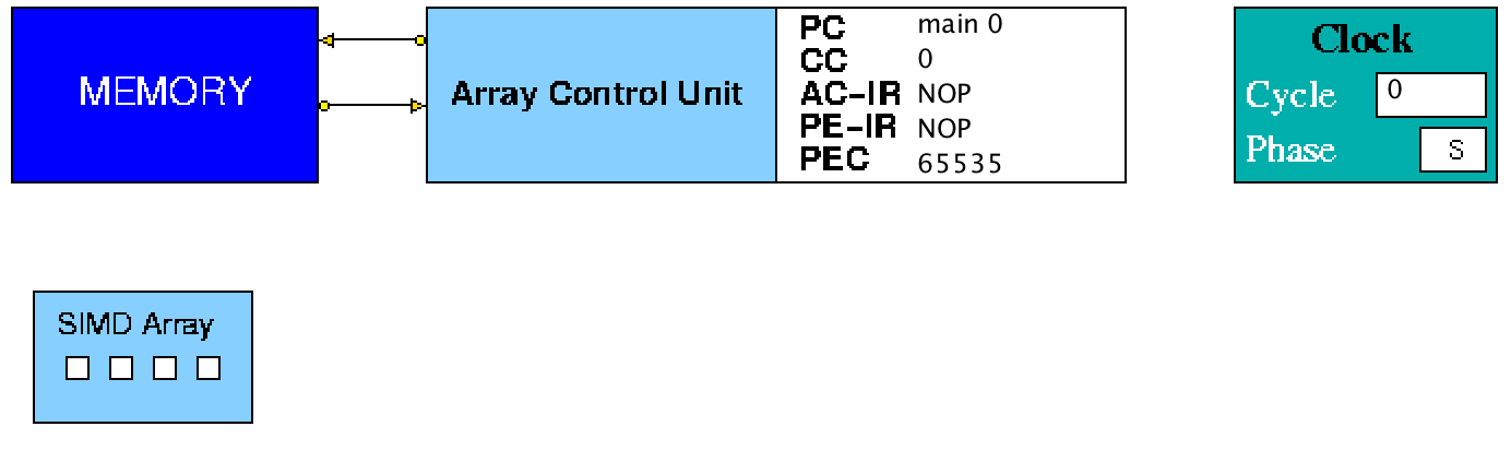
Figure 1. The SIMD-1 simulation model loaded into HASE
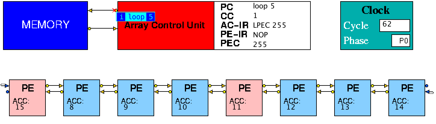
Figure 2. The SIMD-1 simulation model during animation
The SIMD-2 Model
Figure 3 shows the initial image seen when the model is loaded into
HASE. The array is opened for viewing by left clicking in its
icon. Figure 4 shows an image taken during animation of a simulation.
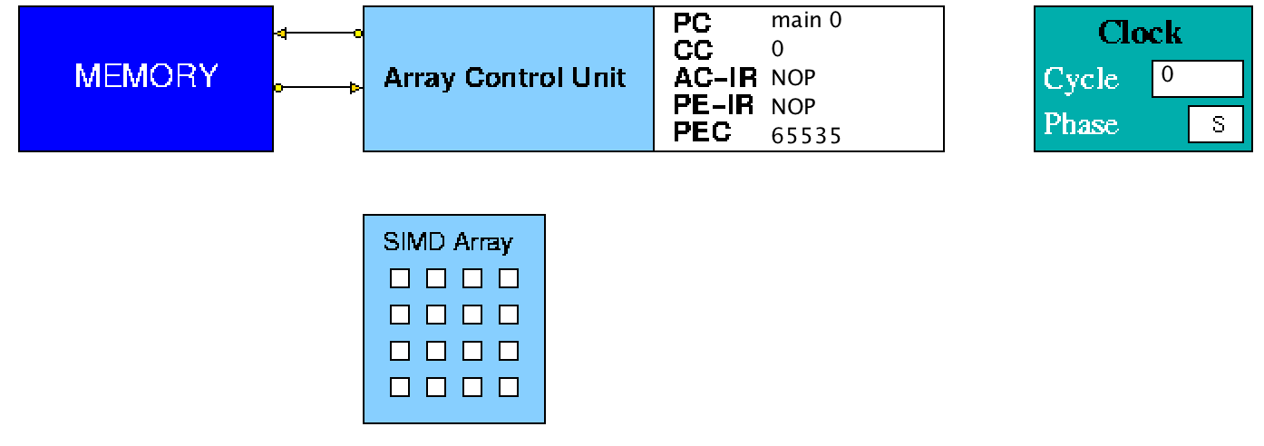
Figure 3. The SIMD-2 simulation model loaded into HASE
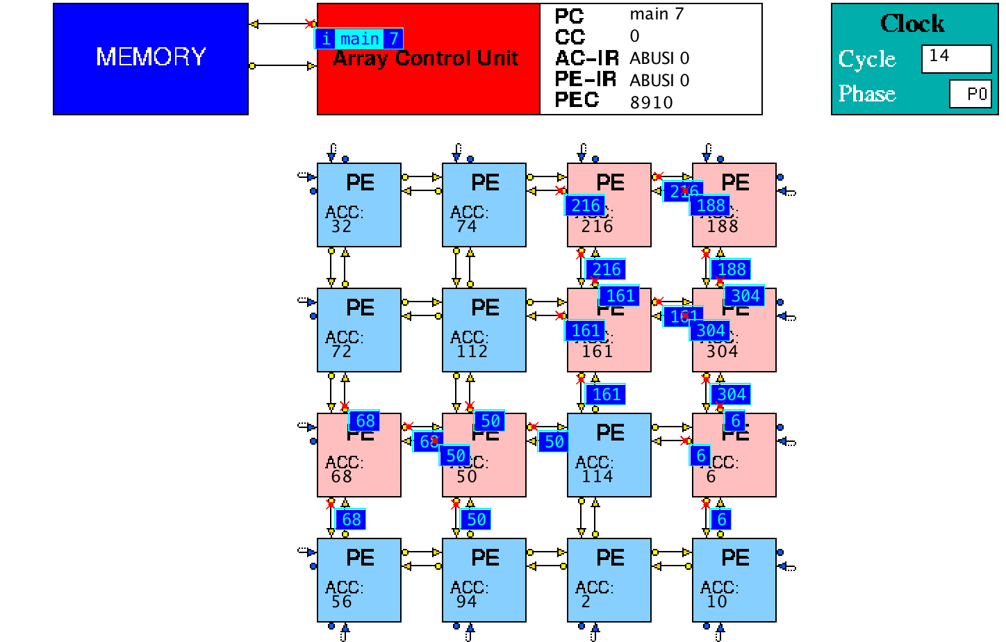
Figure 4. The SIMD-2 simulation model during animation
System Operation
The systems operates on a two phase clock. In clock cycles in which
they are active, each unit executes its internal actions in the first
phase of the clock and sends out a result packet in the second
phase. The Memory, for example, reads an instruction or operand in the
first phase and sends its output to the ACU in the second phase.
The ACU is a simple load/store, register-register arithmetic
processor. It has 16 general purpose registers, a Program Counter
(PC), a Condition code Register (CC) and an Instruction Register
(AC-IR). The Program Counter has two fields: label and offset. The
label field is initially set to "main" and the offset to zero. The ACU
also uses two other registers, the Processing Element Instruction
Register (PE-IR) and the Processing Element Control register (PEC)
which are global registers used to communicate with the SIMD
Array. The Processing Elements operate in lock step, i.e. each
active PE (determined by the state of its PEC bit) obeys the same
instruction at the same time. Whenever a PE ACC is updated by a PE
instruction, the PE sends the new ACC value to each of its neighbours.
The ACU Instruction Set
Table 1 shows the instruction set of the ACU. It includes absolute
jumps (JUMP and JREG) a relative branch (BRANCH), loads (LD, LDL, LDX)
and stores (ST and STX), a move instruction (MOV) which allows values
to be transferred between the ACU registers and the PE Accumulators,
register-register operations (ADD, etc) and register-literal
arithmetic operations (ADDL, etc). All Literal (Immediate) operands
are treated as 16-bit signed integers,
i.e. any literal values which require >16 bits for their
representation are truncated and sign extended to the 32-bit
representation used by the adders.
| INSTRUCTION | ACTION |
| JUMP I | PC = main/Immediate |
| JREG RS | PC = main/(RS) |
| SEQ RS1 RS2 | SET CC if RS1 = RS2 |
| SNE RS1 RS2 | SET CC if RS1 != RS2 |
| SGT RS1 RS2 | SET CC if RS1 > RS2 |
| SLT RS1 RS2 | SET CC if RS1 < RS2 |
| SGE RS1 RS2 | SET CC if RS1 >= RS2 |
| SLE RS1 RS2 | SET CC if RS1 <= RS2 |
| BRANCH Label | if CC = 1, PC = Label/0
if CC = 0 PC = PC + 1 |
| LDI RD I | RD = Immediate |
| LDM RD Rx Address | RD = Memory[Address + (Rx)] |
| STM RS Rx Address | RS => Memory[Address + (Rx)] |
| LPEC I | PEC = Immediate |
| IPEC | Invert PEC bits |
| ALDR RS | PE ACC = RS |
| MOV RD RS | RD = RS |
| MOV RD AS | RD = AS |
| MOV AD RS | AD = RS |
| MOV RD P | RD = PEC |
| MOV P RS | PEC = RS |
ADD RD RS1 RS2
e.g. ADD R1 R2 R3 | RD = RS1 + RS2 |
|
| INSTRUCTION | ACTION |
ADDI RD RS1 I
e.g. ADD R1 R2 42 | RD = RS1 + Immediate |
| SUB RD RS1 RS2 | RD = RS1 - RS2 |
| SUBI RD RS1 I | RD = RS1 - Immediate |
| MUL RD RS1 RS2 | RD = RS1 * RS2 |
| MULI RD RS1 I | RD = RS1 * Immediate |
| DIV RD RS1 RS2 | RD = RS1 / RS2 |
| DIVI RD RS1 I | RD = RS1 / Immediate |
| AND RD RS1 RS2 | RD = RS1 & RS2 |
| ANDI RD RS1 I | RD = RS1 & Immediate |
| OR RD RS1 RS2 | RD = RS1 | RS2 |
| ORI RD RS1 I | RD = RS1 | Immediate |
| XOR RD RS1 RS2 | RD = RS1 ^ RS2 |
| XORI RD RS1 I | RD = RS1 ^ Immediate |
| SLL RD RS1 RS2 | RD = RS1 << RS2 |
| SLLI RD RS1 I | RD = RS1 << Immediate |
| SRL RD RS1 RS2 | RD = RS1 >> RS2 |
| SRLI RD RS1 I | RD = RS1 >> Immediate |
| SRA RD RS1 RS2 | RD = RS1 >> RS2 |
| SRAI RD RS1 I | RD = RS1 >> Immediate |
| NOP | No Operation |
| STOP | Stops the simulation |
|
Table 1. ACU instruction set
JUMP Literal
JUMP takes a Literal (Immediate) operand which is loaded into the
offset field of PC as an absolute instruction address; the label field
of PC is set to "main". The value in PC is then sent to the Memory.
JREG RS
JREG uses a single source register (RS), the contents of which are
read and loaded into the offset field of PC as an absolute instruction
address; the label field of PC is set to "main". The value in PC is
then sent to the Memory.
Compare Instructions
Compare instructions (SEQ, SNE, SGT, SLT, SGE, SLE) compare the values
in registers RS1 and RS2 and set CC accordingly.
BRANCH
BRANCH takes a label as its operand. If CC = 1, the label is loaded
into the label field of PC while the offset field is set to 0; if CC =
0, the offset field of PC is incremented. The value in PC is then sent
to the Memory.
LDL RD Literal
LDL loads the value in the Literal field into the destination register
(RD).
LDM RD Rx Address
LDM adds the value held in register Rx to the value in the Address
field, sends the result to the Data Memory and loads the value
received from the Memory into the destination register (RD).
STM RS Rx Address
STX adds the value in register Rx to the value in the Address
field, then sends this address to Memory together with the value in
source register RS.
LPEC Literal
LPEC loads the value in the Literal field into the PE Control
Register. It’s convenient to specify the Literal in hex format in the
instruction (e.g. 0xff in SIMD-1 or 0xffff in SIMD-2 to set all
the processors active), though it will be displayed in decimal in the
Instruction Register (AC-IR).
ALDR RS
The ACU sets the function in PE-IR to ALDI and copies the value in RS
to the Immediate field in PE-IR. Those PEs that have their PE control
bit set to active then execute the ALDI instruction.
ALDR Address(RS)
The ACU sets the function in PE-IR to ALDM and copies the value of
Address plus the value in RS to the Address field in PE-IR. Those
PEs that have their PE control bit set to active then execute
the ALDM instruction.
MOV
MOV allows values to be moved from one R register to another,
between an R register and the Accumulator of one of the Processing
Elements in the array, or between an R register and PEC. Other
combinations will cause the simulation to stop.
- MOV RD RS : moves the value in RS to RD
- MOV RD AS : moves the value in the ACC of the PE specified by AS to RD
- MOV AD RS : loads the value in RS into the ACC of the PE specified by AS
- MOV RD P : loads RD with the value in PEC
- MOV P RS : loads PEC with the value in RS
Aritmetic Operations
ADD/ADDL adds the values in RS1 and RS2/Literal and writes the
result into RD.
SUB/SUBL subtracts the value in RS2/Literal from the value in RS1
and writes the result into RD.
MUL/MULL multiplies the values in RS1 and RS2/Literal and writes the
result into RD.
DIV/DIVL divides the value in RS1 by RS2/Literal and writes the
result into RD.
AND/ANDL ands the values in RS1 and RS2/Literal and writes the
result into RD.
OR/ORL ors the values in RS1 and RS2/Literal and writes the result
into RD.
XOR/XORL xors the values in RS1 and RS2/Literal and writes the
result into RD.
Shift Instructions
SLL and SLLL (Shift Left Logical) shifts left the value in RS1
by the number of places specified in RS2 (SLL) or the Literal (SLLL)
and writes the result into RD.
SRL and SLRL (Shift Right Logical) shifts right the value in
RS1 by the number of places specified in RS2 (SRL) or the Literal
(SRLL), inserting zeros into digits to the left of the most
significant bit; the result is written into RD.
SRA and SRAL (Shift Right Arithmetic) shifts right the value in
RS1 by the number of places specified in RS2 (SRA) or the Literal
(SRAL), copying the sign digit into digits to its left; the result is
written into RD.
STOP stops the simulation.
The Array Processing Element Instruction Set
Table 2 shows the instruction set of the Processors in the Array. The
processors take their instructions from the Instruction Register
(PE-IR), which is loaded by the ACU. Instructions are divided into
Arithmetic/Logical instructions and PE Control Setting
instructions. The Arithmetic/Logical instructions are further divided
into three subgroups with opcodes of the
form Opcode, OpcodeI
and OpcodeM. All are single address instructions which
combine the value in their Accumulator (ACC) with an input Operand and
return the result to their own ACC. At the end of an operation which
updates the ACC, each active PE sends the value in its Accumulator to
its neighbours.
In the SIMD-1 model the source of the Operand for an Opcode
instructions can be E0, E1, W0, W1 or P,
while in the SIMD-2 model the Operand can be
N0, N1, E0, E1, W0, W1, S0, S1 or P, where an
| N |
Operand = value sent by processor above |
| E |
Operand = value sent by processor to the right |
| W |
Operand = value sent by processor to the left |
| S |
Operand = value sent by processor below |
| P |
Operand = Processor’s own number within the array (0-7 in SIMD-1,
0-15 in SIMD-2) |
and where 0 and 1 indicate the Wraparound condition:
| N0/E0/W0/S0 |
a PE at the end of a row/column uses zero as its operand |
| N1/E1/W1/S1 |
a PE at the end of a row/column uses the value sent from the PE at the other end of the row/column |
For an OpcodeI instruction, the Operand is the Immediate value
in PE-IR.
For and OpcodeM instruction, the ACU reads the value
in Rx from within its own Registers, adds this to the value in the
Address field in AC-IR and loads this modified value into the address
field of the instruction as it is copied into PE-IR. Each Processing
Element accesses its own memory to obtain the operand using the
modified address in PE-IR, i.e. it ignores the Rx field.
PE Control Setting Instructions are of the OpcodeI type.
When executing these instructions, each PE sets its own control bit in
the PE Control Register (PEC) according to the condition selected
by the Opcode
| Arithmetic/Logical Instructions |
| INSTRUCTION | ACTION |
| ALD | ALDI | ALDM | ACC = Operand |
| AADD | AADDI | AADDM | ACC = ACC + Operand |
| ASUB | ASUBI | ASUBM | ACC = ACC - Operand |
| ABUS | ABUSI | ABUSM | ACC = Operand - ACC |
| AMUL | AMULI | AMULM | ACC = ACC * Operand |
| ADIV | ADIVI | ADIVM | ACC = ACC / Operand |
| AVID | AVIDI | AVIDM | ACC = Operand / ACC |
| AAND | AANDI | AANDM | ACC = ACC & Operand |
| AOR | AORI | AORM | ACC = ACC | Operand |
| AXOR | AXORI | AXORM | ACC = ACC ^ Operand |
| ASLL | ASLLI | ASLLM | ACC = ACC << Operand |
| ASRL | ASRLI | ASRLM | ACC = ACC >> Operand |
| ASRA | ASRAI | ASRAM | ACC = ACC >> Operand |
| --- | --- | ASTM | ACC => Operand |
|
| PE Control Setting Instructions |
| INSTRUCTION | CONDITION |
| ASEQ | ACC = Immediate |
| ASNE | ACC != Immediate |
| ASGT | ACC > Immediate |
| ASLT | ACC < Immediate |
| ASGE | ACC >= Immediate |
| ASLE | ACC <= Immediate |
|
Table 2 Array Element instruction set
Using the SIMD-1 Model
When first loaded, the model contains a program (Figure 5) that
reverses the order of the values held in memory locations 0 and 2 of
the Processing Elements and leaves the results in location 1 and 3 of each of
their memories, i.e. it moves the data in memory locations 0
and 2 of PEs 0-7 into memory locations 1 and 3 of PEs 7-0.
The files for the SIMD-1 model include:
MEMORY.instr_mem.mem
MEMORY.data_mem.mem | the initial contents
of the ACU Instruction and
Data memories contained within the Memory Unit |
| ACU.main_reg.mem | the initial contents of the ACU registers;
this file should not be edited |
| SIMD1.pe1.pe_mem.mem | the initial contents of the PE memories |
Because the SIMD Array of processing elements (SIMD1) is defined as a
mesh (MESH1D in the simd-1.edl file), HASE automatically loads the
memories in the SIMD1 array from the SIMD1.pe1.pe_mem.mem
file. This file has the following form:
| 0 |
| 0 |
| 8 |
| 0 |
| //$next section |
| 1 |
| 0 |
| 9 |
| 0 |
| //$next section
|
Thus the first four values are loaded into locations 0-3 of PE0’s
memory, the second four into locations 0-3 of PE1’s
memory, etc.
| LDI R1 0 | // R1 is used as an index into the PE memory |
| LDI R2 4 | // R2 is used as the limiting index value |
| loop: | // |
| ALDM R1 0 | // load data into ACCs |
| ALD W1 | // load data from west neighbour |
| LPEC 0x88 | // load PE Control register |
| ASTM R1 1 | // Write data to memories of selected PEs |
| LPEC 0xFF | // |
| ALD W1 | // |
| ALD W1 | // |
| LPEC 0x44 | // |
| ASTM R1 1 | // |
| LPEC 0xFF | // |
| ALDM R1 0 | // |
| ALD E1 | // |
| LPEC 0x11 | // |
| ASTM R1 1 | // |
| LPEC 0xFF | // |
| ALD E1 | // |
| ALD E1 | // |
| LPEC 0x22 | // |
| ASTM R1 1 | // |
| LPEC 0xFF | // |
| ALDM R1 1 | // |
| ADDI R1 R1 2 | // |
| SLT R1 R2 | // test for limiting index value |
| BRANCH loop | // |
| STOP | // |
Figure 5. SIMD-1 Demonstration Program Code
To run a new program, edit MEMORY.instr_mem.mem and, if
appropriate, MEMORY.data_mem.mem and
SIMD1.pe1.pe_mem.mem. Then just press run. The new contents of
the memories will appear in the parameters panel as the locations are
accessed during animation. To get the values to appear immediately,
re-load the model after closing the edits.
Suggested Student Exercise
For the SIMD-1 Array Processor model, write an assembly code program,
together with appropriate data in the PE memories, that loads 0 into
the ACC of processor 0, 1 into the ACC of processor 1, etc, and then
forms the set of parallel pre-fix sums for these numbers. You can load
the ACCs from memory or by using the own processor number facility in
the instruction set.
Your submission for this part should consist of three documents:
- a commented listing of the program
- an uncommented listing of the program suitable for copying and
pasting into the ACU memory file (so that the instructor can run it)
- a text file containing a note of the number of simulated clock
cycles your program took to execute and comments on the degree of
parallelism during its execution.
Using the SIMD-2 Model
When first loaded, the model contains the program shown in Figure
6. The first instruction loads each PE ACC with the PE’s own number in
the array. The second instruction loads each PE ACC with the value in
word 0 of its memory, in this case equal to the process number, so the
result should be 0 in each ACC. The next four instructions load the
ACC with the value in word 1, multiply it by the value in word 2,
subtract the value in word 3 and then set the PE Control bit if the
result is negative. The next instruction (Reverse Subtract) is only
executed in PEs with a negative ACC (making their ACC values
positive). Finally, the PE control bits are all set to 1 and all ACC
values are written to memory word 4.
The files for the SIMD-2 model include:
MEMORY.instr_mem.mem
MEMORY.data_mem.mem |
the initial contents of the ACU Instruction and
Data memories contained within the Memory Unit |
| ACU.main_reg.mem |
the initial contents of the ACU registers;
this file should not be edited |
| SIMD2.pe2.pe_mem.mem |
the initial contents of the PE memories |
Similarly to the SIMD1 Array, the SIMD Array of processing elements
(SIMD2) is defined as a mesh (MESH2D in the simd-2.edl file), HASE
automatically loads the memories in the SIMD2 array from
the SIMD2.pe2.pe_mem.mem file has the same form
as SIMD1.pe1.pe_mem.mem, so the first four values are loaded
into locations 0-3 of PE0’s memory, the second four into
locations 0-3 of PE1’s memory, etc. Note that the PEs are
numbered in column order.
| ALD P | // load ACC with PE’s own number |
| ASUBM R0 0 | // subtract value in memory word 0 from ACC |
| ALDM R0 1 | // load ACC from memory word 1 |
| AMULM R0 1 | // multiply by value in memory word 2 |
| ASUBM R0 3 | // subtract value in memory word 3 |
| ASLT 0 | // set PE Control bit if ACC -ve |
| ABUSI 0 | // negate value in ACC |
| LPEC 0xFFF | // set all PE Control bits |
| ASTM R0 4 | // write ACC value to memory word 4 |
| STOP | |
Figure 6. SIMD-2 Demonstration Program Code
Suggested Student Exercise
Figure 7 shows a data file suitable for use as a
SIMD2.pe2.pe_mem.mem file. Copy this data into the file of this name
in your copy of the SIMD-2 model files. For each PE, locations 1-4 and
5-8 contain elements of vectors A and B respectively. Write an
assembly code program for SIMD-2 which first of all forms the scalar
product of these two vectors, leaving the result in location 0 of the
memory of each PE. The program should then form the sum of (a) all the
positive scalar product results (copying this result into ACU Register
3) (b) the sum of all the negative scalar product results (copying
this result into ACU Register 4).
Your submission for this part should consist of four documents:
- a commented listing of the program
- an uncommented listing of the program suitable for copying and
pasting into the ACU memory file (so that the instructor can run it)
- a listing of the contents of the ACU registers at the end of the program
- a text file containing a note of the number of simulated clock
cycles your program took to execute and comments on the degree of
parallelism during its execution
0
1
2
3
4
5
6
7
8
0
//$next section
0
9
10
11
12
-13
14
15
-16
0
//$next section
0
17
18
19
20
21
22
23
24
0
//$next section
0
25
26
27
28
29
-30
31
-32
0
//$next section
0
33
34
35
36
37
38
38
40
0
//$next section
0
41
-42
43
44
45
46
47
-48
0
//$next section
0
49
50
51
52
53
54
55
56
0
//$next section
0
-57
58
59
60
61
62
63
-64
0
//$next section
0
65
66
-67
68
69
70
71
72
0
//$next section
0
73
74
75
76
77
78
79
80
0
//$next section
0
81
82
-83
84
85
86
87
-88
0
//$next section
0
89
90
91
92
93
94
95
96
0
//$next section
0
97
98
99
100
101
102
103
104
0
//$next section
0
105
106
107
-108
-109
110
111
112
0
//$next section
0
113
114
115
116
117
-118
119
120
0
//$next section
0
121
122
123
124
125
126
-127
-128
0
|
Figure 7. Data file for SIMD-2 Exercise
Return to Computer Architecture Simulation Models
HASE Project
Institute for Computing Systems Architecture, School of Informatics,
University of Edinburgh
Last change 25/01/2024